Signal and Power Integrity
Good signal and power integrity are critical in order to get the best performance possible from your PCB design or system. No two analysis requirements are the same and which one(s) you employ depends upon the task at hand. Below are examples of the types of analysis most commonly carried out on our clients’ designs.
Power-Aware Signal Integrity Analysis. Analysis tools have historically treated signal integrity and power integrity separately. The two are inextricably linked and should usually be carried out simultaneously to avoid over-optimistic results. PASI analysis allows visibility of how signals are going to behave as they traverse IC packages, PCB traces, vias, connectors, passive components, etc.

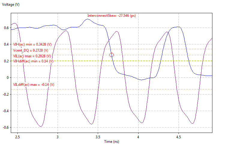
Memory Controller Sign-Off. For a DDR memory interface to be compliant it must satisfy many SI and timing specifications. The memory compliance tools stream-line this process and provide a set of reports highlighting any weaknesses in the memory controller.
This information may be used to improve the PCB layout, modify termination schemes and to re-assess the internal settings used within the SDRAM and memory controller ICs (drive strengths, ODT, etc).
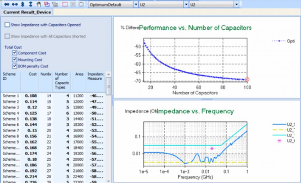
Capacitor Optimisation. The capacitor optimisation tools allow rapid analysis of thousands of capacitor fitment combinations, often resulting in the removal of many unnecessary ceramic capacitors.
This analysis measures the power impedance at specific ICs and takes into account the entire power delivery network, including planes, vias, traces and capacitor models. The tool aims to meet the necessary impedance whilst achiving a capacitor goal, which could be cheapest bill of materials, smallest area, fewest devices, etc.
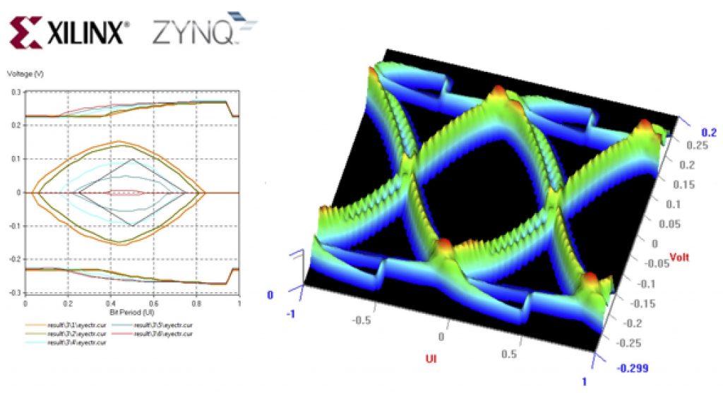
Channel Analysis is a methodology that allows millions of bit transitions to be simulated in a multi-gigabit SERDES channel, allowing the channel’s bit error rate (BER) to be quantified. IBIS-AMI models from vendors including Xilinx and Intel allow channels to be simulated using accurate behavioural descriptions of the SERDES transceivers being employed. Optimum TX/RX settings may be found by exploring gain, emphasis and equalisation settings deep within the SERDES block.
DC Power Analysis. IC core power supplies continue to demand higher currents, placing greater demands on printed circuit power structures. Power analysis allows modelling of these DC interconnections, highlighting excessive current densities, hot-spots and IR-drop. Power delivery networks can quickly be evaluated to ensure sufficient via barrels, copper cross-sections, etc. exist to carry the required current and without losing too much power in the PCB as heat (a serious consideration on battery-life critical hardware).
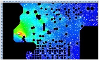
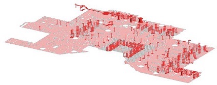
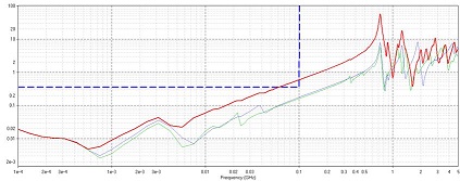
AC Power Analysis. Power delivery networks (PDNs) can involve extremely complicated PCB layout in order to connect the power supply to the power and ground pins of ICs. The electrical behaviour of the PDN will be affected by many things, including vias, traces, plane shapes, voids, inter-plane capacitance, capacitor types/values, capacitor mounting parasitics and PCB stack-up.
Impedance profiles are extracted from the printed circuit design to measure the performance of the power delivery networks. This view allows us to ‘look into’ the power planes from the ICs’ perspective and gauge whether or not the design is suitable for operation.
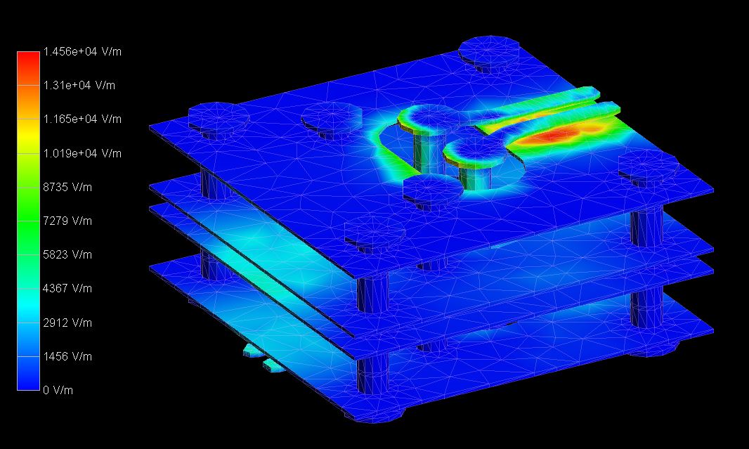
3D-FEM Analysis can be used to perform accurate full-wave modelling of PCB structures. The finite element method will solve 3D structures in great detail, allowing the subtleties of the layout to be considered for very high-speed signal paths.
- Optimise via transitions
- Minimise return losses in MGbit I/Os
- Optimise MGbit compliance (e.g. SMPTE 4K, etc.)
- Optimise MGbit, RF and µwave layouts
